郭国娜透射电镜和扫描电镜都有哪些应用领域呢英语
- tem电镜样品
- 2024-04-25 20:30:20
- 71
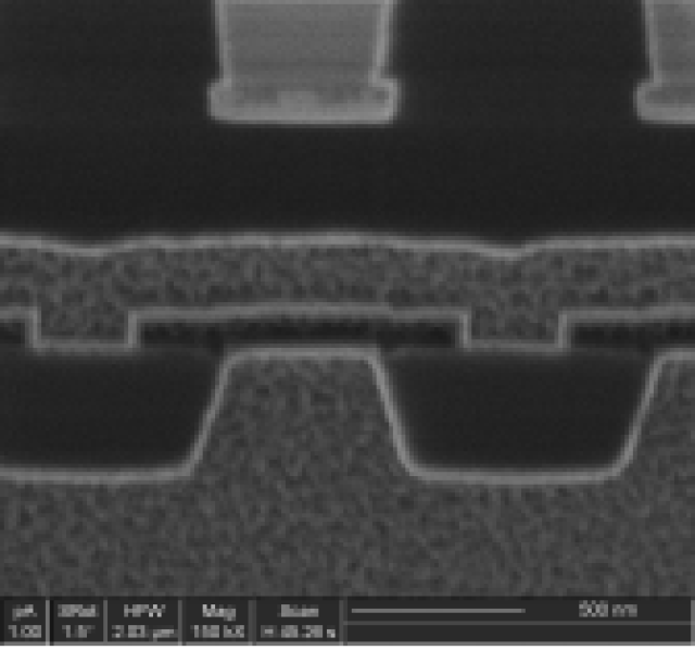
纳瑞科技的服务将为IC芯片设计工程师、IC制造工程师缩短设计、制造时间,增加产品成品率。我们将为研究人员提供截面分析,二次电子像,以及透射电镜样品制备。我们同时还为聚焦离子束系统的应用客户提供维修、系统安装、技术升级换代、系统耗材,以及应用开发和培训。
Transmission electron microscopy and scanning electron microscopy are two important microscopy techniques that have various applications in different fields. Transmission electron microscopy is a research technique that uses a high-energy beam of electrons to visualize the internal structure of materials. It is commonly used to study the physical properties of materials, such as their strength, conductivity, and optical properties.

Scanning electron microscopy, on the other hand, is a non-invasive imaging technique that uses a beam of electrons to create a detailed map of the surface of a material. It is widely used to study the chemical composition and surface structure of materials. The technique can be used to examine the surface of a material to identify various features such as atoms, vacancies, and other defects.
Both transmission electron microscopy and scanning electron microscopy have their own unique applications in various fields. Here are some examples of the applications of these techniques:
Transmission electron microscopy:
1. Materials science: Transmission electron microscopy is widely used to study the physical properties of materials. It is particularly useful for studying the strength, conductivity, and optical properties of materials.
2. Conditional testing: This is a technique that involves exposing materials to different conditions, such as high-temperature or high-pressure. Transmission electron microscopy can be used to study the effects of these conditions on the material's structure and properties.
3. Defect analysis: Transmission electron microscopy can be used to identify defects in materials, such as vacancies or dislocation. These defects can have a significant impact on the material's properties, and analysis by transmission electron microscopy can help to understand their formation and behavior.
Scanning electron microscopy:
1. surface analysis: Scanning electron microscopy is commonly used to study the surface structure of materials. It can be used to identify various features such as atoms, vacancies, and other defects, which can have a significant impact on the material's properties.
2. chemical analysis: Scanning electron microscopy can be used to study the chemical composition of materials by analyzing the energy absorption spectrum of the electrons. This can provide information about the presence and type of chemical bonds on the surface of the material.
3. physics: Scanning electron microscopy can be used to study the structure and properties of thin films and other surfaces. It can be used to study the behavior of surface electrons and their interactions with other particles.
In conclusion, transmission electron microscopy and scanning electron microscopy are two important microscopy techniques that have various applications in different fields. These techniques can be used to study the physical properties of materials, their surface structure, and chemical composition. Further research in these areas can lead to new and improved technologies for various industries.
郭国娜透射电镜和扫描电镜都有哪些应用领域呢英语 由纳瑞科技tem电镜样品栏目发布,感谢您对纳瑞科技的认可,以及对我们原创作品以及文章的青睐,非常欢迎各位朋友分享到个人网站或者朋友圈,但转载请说明文章出处“透射电镜和扫描电镜都有哪些应用领域呢英语 ”

下一篇
扫描电镜检测标准